
Before the actual assembly process, the manufacturer should thoroughly check the PCB design documents to check its function and manufacturability. This stage is called DFM. It checks the design specifications of the PCB and analyzes any missing, redundant or potentially problematic features. This stage helps to detect design errors and allows designers to remove all defects immediately, leading to successful production.
Start the actual PCB assembly process
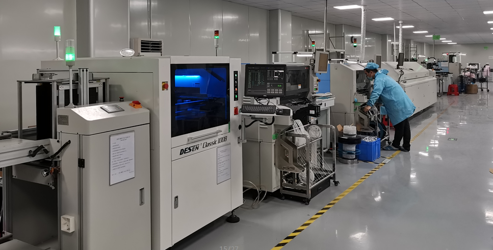
Now start the actual PCB assembly process as described below.
1. Application of solder paste: First, apply solder paste (a small particle of solder paste mixed with flux) on the board. For this application, most PCB manufacturers use stencils (there are several sizes, shapes and specifications are consistent with the specifications), these stencils can only correctly apply the correct amount of solder paste to certain parts of the board.
2. Component placement: Unlike the past, the PCB assembly process at this stage is now fully automated. Picking and placing of parts (such as surface mount components) was once done manually, but now it is performed by robotic pick and place machines. These machines accurately place components on the pre-planned area of the circuit board.
3. Reflow: Now, the solder paste and all surface mount components are in place. What do you do next? Curing the solder paste to the correct specifications is essential for the proper adhesion of PCB components to it. This is the relevant part of the PCB assembly process-reflow soldering. To this end, the components with solder paste and the components on them are passed through a conveyor belt, and the conveyor belt is passed through an industrial-grade reflow oven. The heater in the oven melts the solder in the solder paste. Once melting is complete, the components will again move on the conveyor belt and be exposed to a series of cooler heaters. The purpose of these coolers is to cool the molten solder and solidify it.
4. Inspection: After the reflow process, the PCB should be inspected to check its function. This stage can help identify poor quality connections, misplaced components, and short circuits due to the continuous movement of the circuit board during the reflow process. PCB manufacturers have adopted multiple inspection steps, such as manual inspection, automatic optical inspection and X-ray inspection, to check the function of the circuit board, identify lower quality solder and find any potential hidden dangers. After the inspection is completed, the assembly team will make a crucial decision. Circuit boards with several functional errors are usually scrapped. On the other hand, if there is a minor error, send the board again for rework.
5. Through-hole component insertion: certain types of PCBs need to be inserted into through-hole components together with conventional SMD components. This stage is dedicated to the insertion of such components. To this end, which PCB components are used to transmit signals from one side of the board to the other to create plated through holes. PCB through-hole insertion usually uses manual or wave soldering to obtain results.
6. Final inspection: Now is the time for the second level inspection. Here, perform a functional test on the assembled board, or perform a thorough inspection on the PCB to monitor its electrical characteristics, including voltage, current, or signal output. Today's manufacturers use a variety of advanced testing equipment to help determine the success or failure of finished boards.
7. Cleaning: Since the soldering process will leave a large amount of flux residue in the PCB, it is important to thoroughly clean the components before the final circuit board is delivered to the customer. For this, the PCBs are washed in deionized water. After the cleaning process, use compressed air to thoroughly dry the board. Now the PCB assembly can be prepared for customer inspection and inspection.
Although the PCB assembly process steps of all types of circuit boards are almost the same, there are still some changes in THT assembly, SMT assembly and hybrid technology. Let us end the discussion by listing the assembly steps for THT, SMT and hybrid boards.
Through-hole technology (THT) assembly steps
1. Component placement
2. Inspection and correction
3. Wave soldering
Steps in surface mount (SMT) assembly
1. Solder paste printing
2. Component installation
3. Reflow soldering
Steps in hybrid assembly
l Single-sided hybrid components
1. Solder paste printing
2. SMD parts placement
3. Reflow soldering
4. THT component placement
5. Wave soldering
SMT on one side and THT on one side
1. Surface mount adhesive
2. SMD parts placement
3. Solidification
4. Flip
5. THT component placement
6. Wave soldering
Double-sided mixed
1. Solder paste printing
2. SMD parts placement
3. Reflow soldering
4. Flip
5.SMT glue
6. SMD parts placement
7. Solidification
8. Flip
9. THT component placement
10. Wave soldering
Now, you must have a good understanding of the basic steps involved in the PCB assembly process. However, depending on the complexity of the project, these steps may also change. For custom PCBs, the modification is more obvious.

Отсканируйте QR-код с помощью WhatsApp

Отсканируйте QR-код с помощью Telegram
WeChat
Отсканируйте QR-код с помощью WeChat