
SMT is a surface mount technology that is the process of placing electronic components on a PCB. How much do you know about the electronic components on the PCB? Let's take a look!
SMC: Surface Mounted commponents
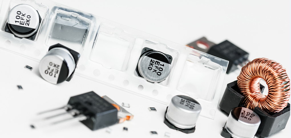
There are mainly rectangular chip components, cylindrical chip components, composite chip components, and shaped chip components.
SMD: Surface Mounted Devices
There are mainly chip transistors and integrated circuits, and integrated circuits include SOP, SOJ, PLCC, LCCC, QFP, BGA, CSP, FC, MCM, and so on. Examples are as follows:
1. Interconnect: Provides mechanical and electrical connection/disconnection, consists of connecting plugs and sockets, connecting cables, brackets, chassis or other PCBs to the PCB; however, the actual connection to the board must be through surface mounting Type contact.
2, active electronic components (Active): In analog or digital circuits, you can control the voltage and current to generate gain or switching, that is, respond to the application of signals, you can change your basic characteristics. Inactive: Provides a simple, repeatable response when the electrical signal is applied without changing its characteristics.
3. Odd-form: The geometry factor is peculiar, but it does not have to be unique. Therefore, it must be mounted by hand, and the shape of the outer casing (compared to its basic function) is not standard.
For example: many transformers, hybrid circuit structures, fans, mechanical switch blocks, and so on.
Chip chip resistors, capacitors, etc. Dimensions: 0201, 0402, 0603, 0805, 1206, 1210, 2010, etc. Tantalum capacitors, size specifications:
TANA, TANB, TANC, TANDOST
Transistors, SOT23, SOT143, SOT89, etc.
Melf cylindrical component, diode, resistor, etc.
SOIC integrated circuit, size specification: SOIC08, 14, 16, 18, 20, 24, 28, 32
QFP close-pitch integrated circuit PLCC integrated circuit, PLCC20, 28, 32, 44, 52, 68, 84
BGA Ball Grid Array Package IC, Array Spacing Specifications: 1.27, 1.00, 0.80
CSP integrated circuit, the side length of the component does not exceed 1.2 times the side length of the chip, and the microBGA with array spacing <0.50
SMT noun explanation
Bridge: A solder that connects two conductors that should be electrically connected to each other, causing a short circuit.
Buried via: An electrically conductive connection between two or more inner layers of a PCB (ie, invisible from the outer layer).
C
CAD/CAM system: Computer-aided design uses specialized software tools to design printed circuit structures; computer-aided manufacturing converts this design into actual products. These systems include large-scale memory for data processing and storage, input for design creation, and output devices for converting stored information into graphics and reports.
Capillary action: A natural phenomenon in which molten solder flows against solid surfaces that are close to each other against gravity.
Chip on board: A hybrid technology that uses chip components that are glued face up, traditionally connected to the base layer of the board by flying leads.
Circuit tester: A method of testing a PCB during mass production. Includes: needle bed, component lead footprints, pilot probes, internal traces, loading plates, empty plates, and component testing.
Cladding: A thin layer of metal foil bonded to the board layer to form PCB conductive traces.
Coefficient of the thermal expansion: When the surface temperature of the material increases, the measured mass per unit of temperature expands in parts per million (ppm).
Cold cleaning: An organic dissolution process in which liquid contact completes the residue removal after soldering.
Cold solder joint: A solder joint that reflects insufficient wetting. It is characterized by a grayish and porous appearance due to insufficient heating or improper cleaning.
Component density: The number of components on the PCB divided by the area of the board.
Conductive epoxy: A polymeric material that passes an electric current by adding metal particles, usually silver.
Conductive ink: A glue used on thick film materials to form a PCB conductive wiring pattern.
Conformal coating: A thin protective coating applied to PCBs that conform to the assembled shape.
Copper foil: A thin, continuous metal foil deposited on the base layer of a circuit board as an electrical conductor of a PCB. It is easy to adhere to the insulating layer, accepts a printed protective layer, and forms a circuit pattern after etching. Copper mirror test: A flux corrosion test in which a vacuum deposited film is used on a glass plate.
Cure: A change in the physical properties of a material, either by chemical reaction or by a pressure/pressureless reaction to heat.
Cycle rate: A component patch noun used to measure the speed of a machine from picking, positioning, and returning, also known as test speed.
D
Data recorder: A device that measures and collects temperature from a thermocouple attached to a PCB at specific time intervals.
Defect: A component or circuit unit that deviates from a normally accepted feature.
Delamination: separation of the plies and separation between the plies and the conductive cover.
Desoldering: Disassemble the welding components for repair or replacement, including: suction with tin, vacuum (solder pipette) and hot drawing.
Dewetting: The process of covering and retracting the molten solder, leaving an irregular residue.
DFM (design for manufacturing): The method of producing products in the most efficient way, taking into account time, cost and available resources.
Dispersant: A chemical that is added to water to increase its ability to degranulate.
Documentation: Information about assembly, explaining basic design concepts, types and quantities of components and materials, specialized manufacturing instructions, and the latest version. Three types are used: prototypes and a small number of runs, standard production lines and/or production quantities, and government contracts that specify actual graphics.
Downtime: The time at which a device does not produce a product due to maintenance or failure.
Durometer: Measures the rubber or plastic hardness of the blade.
E
Environmental test: A test or series of tests used to determine the overall external impact on the structural, mechanical, and functional integrity of a given component package or assembly.
Eutectic solders: Two or more metal alloys with the lowest melting point. When heated, the eutectic alloy changes directly from solid to liquid without going through the plastic phase.
F
Fabrication(): The empty board manufacturing process prior to assembly after design. The individual processes include lamination, metal addition/subtraction, drilling, plating, routing, and cleaning.
Fiducial: A special mark integrated with a circuit pattern for machine vision to find the direction and position of the wiring pattern.
Fillet: A connection formed by solder between a pad and a component lead. That is, solder joints.
Fine-pitch technology: The surface of the surface mount component package has a center-to-center spacing of 0.025" (0.635mm) or less.
Fixture: A device that connects a PCB to the center of the processing machine.
Flip chip: A leadless structure that typically contains circuit elements. It is designed to be electrically and mechanically connected to the circuit by a suitable number of solder balls (covered by a conductive adhesive) on its face.
Full liquidus temperature: The temperature level at which the solder reaches its maximum liquid state, which is best for good wetting.
Functional test: Simulates the expected operating environment and tests the entire assembled electrical appliance.
G
Golden boy: A component or circuit assembly that has been tested and known to function to meet specifications and is used to test other units by comparison.
H
Halides: Compounds containing fluorine, chlorine, bromine, iodine or hydrazine. It is the catalyst part of the flux and must be removed due to its corrosive nature.
Hard water: Water contains calcium carbonate and other ions that may accumulate on the inner surface of clean equipment and cause blockages.
Hardener: A chemical added to a resin to prematurely cure, ie, a curing agent.
I
In-circuit test: A component-by-component test to verify the placement and orientation of components.
J
Just-in-time (JIT is just on time): Minimize inventory by supplying materials and components directly to the production line before putting it into production.
L
Lead configuration: A conductor that extends from a component and acts as both a mechanical and electrical connection.
Line certification: Confirm that the production line is in a controlled sequence and can produce a reliable PCB as required.
M
Machine vision: One or more cameras used to help find the center of the component or improve the component placement accuracy of the system.
Mean time between failure: The average statistical time interval at which a possible operational unit failure is expected, usually calculated on an hourly basis, and the results should indicate actual, projected, or calculated.
N
Nonwetting: A condition in which solder does not adhere to a metal surface. Due to the contamination of the surface to be welded, the characteristic of non-wetting is the bareness of the visible base metal.
O
Omegameter: A meter used to measure the amount of ionic residue on the surface of a PCB by immersing the assembly in a mixture of alcohol and water of known high resistivity, after which it is measured and recorded as a result of ion residue. The resistivity drops. Open: The two electrical connections (pins and pads) become separate, for reasons that are not soldered enough, or if the junction pins are poorly coplanar.
Organic activated: A fluxing system of organic acids as an active agent, water soluble.
P
Packaging density: The number of components (active/passive components, connectors, etc.) placed on the PCB; expressed as low, medium, or high.
Photoploter: A basic wiring pattern processing device used to produce a master PCB layout (usually the actual size) on a photographic film.
Pick-and-place: A programmable machine that has a robotic arm that picks up components from an automatic feeder, moves to a fixed point on the PCB, and places it in the correct position in the correct orientation. .
Placement equipment: A machine that combines high-speed and accurate positioning of components onto a PCB. There are three types: SMD's mass transfer, X/Y positioning, and online transfer systems that can be combined to adapt components to the circuit. Board design.
R
Reflow soldering: The process of permanently attaching surface mount components to solder paste through various stages including preheating, stabilization/drying, peak reflow and cooling.
Repair: The action to restore the function of a defective assembly.
Repeatability: The process capability to accurately revert back to a feature target. An indicator that evaluates the processing equipment and its continuity.
Rework: Bringing an incorrect assembly back to an iterative process that meets specifications or contract requirements.
Rheology: Describes the flow of a liquid, or its viscosity and surface tension properties, such as solder paste.
S
Saponifier: An aqueous solution of an organic or inorganic major ingredient and additive used to promote the removal of rosin and water soluble fluxes, such as by dispersible cleaners.
Schematic: A diagram that uses symbols to represent the layout of a circuit, including electrical connections, components, and functions.
Semi-aqueous cleaning: Technology involving solvent cleaning, hot water washing and drying cycles.
Shadowing: In infrared reflow soldering, the body of the component blocks energy from certain areas, causing insufficient temperature to completely melt the solder paste.
Silver chromate test: A qualitative, halogenated ion check in the presence of RMA flux. (RMA reliability, maintainability and availability)
Slump: The diffusion of solder paste, glue and other materials before curing after stencil screen printing.
Solder bump: A spherical solder material bonded to the contact area of a passive or active component that acts as a connection to the circuit pad.
Solderability: The ability of a conductor (pin, pad or trace) to become wet (to become solderable) in order to form a strong connection.
Soldermask: The processing technology of printed circuit boards, except that all surfaces except the joints to be soldered are covered by a plastic coating.
Solids: weight percent of rosin in the flux formulation, (solids content)
Solidus: The temperature at which the solder alloy of some components begins to melt (liquefy).
Statistical process control: Analyze process output using statistical techniques to guide actions, adjust and/or maintain quality control status.
Storage life: The time during which the glue is stored and maintained useful.
Subtractive process: The circuit wiring is obtained by removing the conductive metal foil or the selected portion of the cover layer.
Surfactant: A chemical that is added to water to reduce surface tension and improve wetting.
Syringe: A gel container that is dropped through its narrow opening.
T
Tape-and-reel (package and disc): The component package for the patch, on the continuous strip, the component is placed in the pit, the pit is covered by the plastic strip, so as to be wound onto the disc for the component patch Machine use.
Thermocouple: A sensor made of two different metals that produces a small DC voltage during temperature measurement when heated.
Type I, II, III assembly (first, second, and third assembly):
a PCB (I) having surface mount components on one or both sides of the board;
a hybrid technology with a lead component mounted on the main surface and with SMD components mounted on one or both sides (II);
A hybrid technology (III) featuring a passive SMD component mounted on the second side and a pin (through-hole) component mounted on the main surface.
Tombstoning: A soldering defect in which the sheet-like component is pulled to a vertical position so that the other end is not soldered.
U
Ultra-fine-pitch: The center-to-center distance of the pins and the conductor spacing are 0.010” (0.25 mm) or less.
V
Vapor degreaser: A cleaning system that suspends objects in a tank and the heated solvent vapor condenses on the surface of the object.
Void: A cavity formed inside a tin spot formed by the flux remaining before the gas is released or solidified during reflow.
Y
Yield: The ratio of the components used at the end of the manufacturing process to the number of components submitted for production.
Shenzhen Hengtian Weiye Technology Co., Ltd. is a one-stop service company that integrates PCB production, SMT patch, electronic component purchasing and functional testing. The purchase of electronic components can be obtained by contacting the online service.

Отсканируйте QR-код с помощью WhatsApp

Отсканируйте QR-код с помощью Telegram
WeChat
Отсканируйте QR-код с помощью WeChat