
The assembly process of printed circuit boards is relatively cumbersome and requires a lot of processes. Let's take a look at the assembly process of printed circuit boards today.
First, the printed circuit board bare board is transported by the PCB manufacturer to the PCBA manufacturer and enters the SMT workshop.
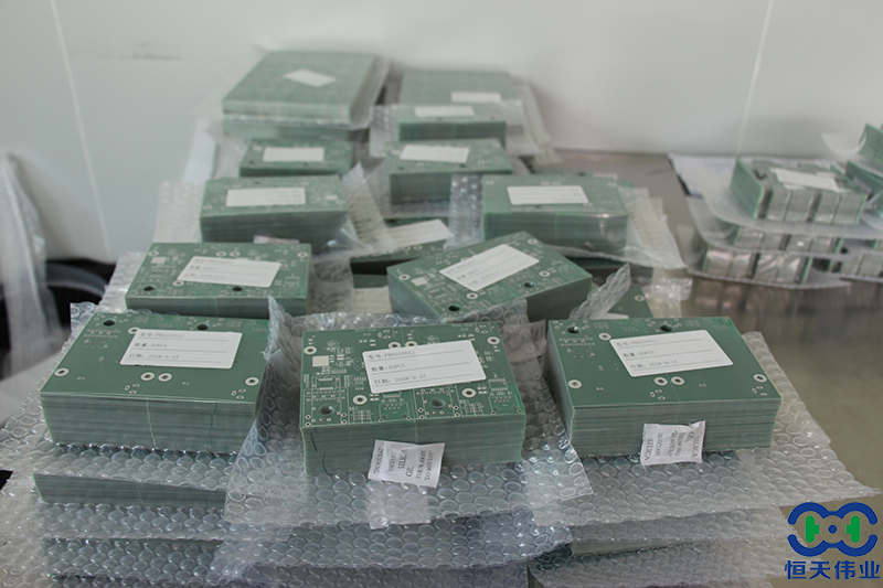
The bare board of the PCB is sent to the SMT equipment for feeding by the board feeder.
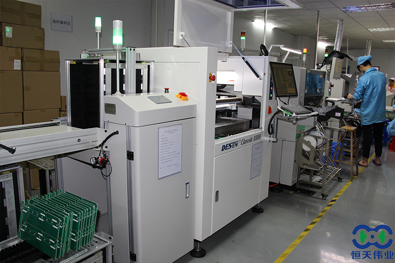
Here, the component placement on the PCB is based on the SMT setting procedure, and the small components are mainly placed on the designated position of the bare PCB.
Detection, generally by manual inspection, to see if there is an error, here generally refers to a large error.
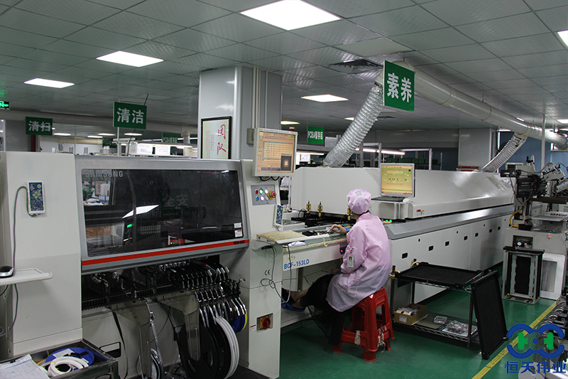
Then, as the transmission line is automatically fed into the wave soldering, the tin is mainly fused to the pad.
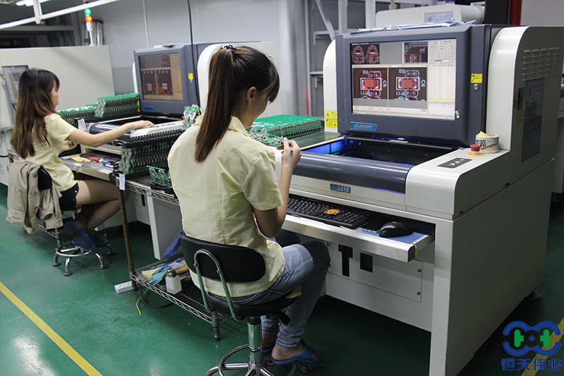
The next process is computer testing. The detection here mainly detects whether there are fewer materials, pads and other related problems.
After the SMT workshop is completed, the PCB semi-finished board is sent to the PCBA assembly line to enter the plug-in process.
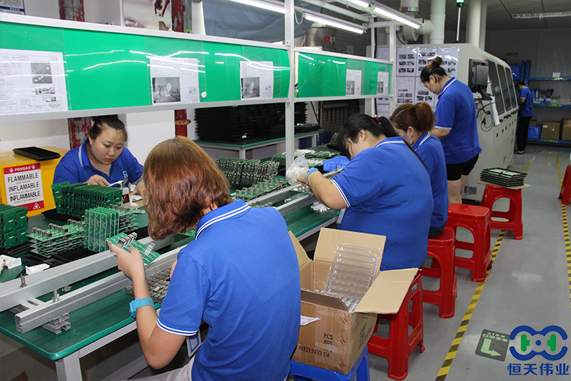
Plug-in, here refers to plugging large components, such as USB interface, large resistance, large LED lights, etc., after inserting the pieces into the wave soldering.
Finally, the function test, before the function test, the program is burned, and then the tool is used for the function test. The PCBA test generally formulates the specific test process according to the customer's test plan. The PCBA test generally includes five main forms: ICT test, FCT test, Aging test, fatigue test, test in harsh environment.
When the functional test is completed, it can be sent directly to the finished assembly shop for assembly, such as mobile phones, computers, Bluetooth stereos, etc. This is the approximate process of printed circuit board assembly.
WeChat
Отсканируйте QR-код с помощью WeChat