
Она предлагает небольшие и средние партии PCB для производства платы на уровне 1 - 32 слоя. Опираясь на 18 - летний опыт производства, он предоставляет высококачественные услуги более чем 100 странам и десяткам тысяч клиентов во всем мире!
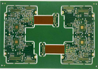
Can produce 1-32 layer PCB board
★ Gold-plated board, OSP board, silver board, gold board, tin board, tin plate
★ FR-4, aluminum substrate, cardboard, semi-glass fiber (CEM-1), etc.
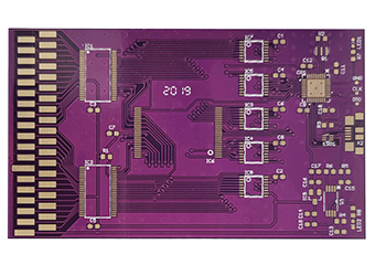
Provide PCB special process custom production services
Strong engineering team support
Advanced production equipment meets process requirements
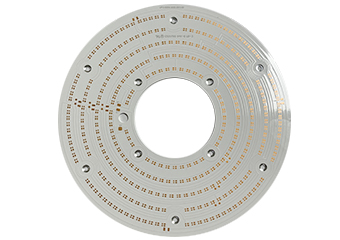
Aluminum substrate/mixed aluminum substrate thermal conductivity 1-3W
★ Aluminum plate + high thermal conductivity insulating material, high thermal conductivity
★ Up to 8 layers of mixed-pressed aluminum substrates
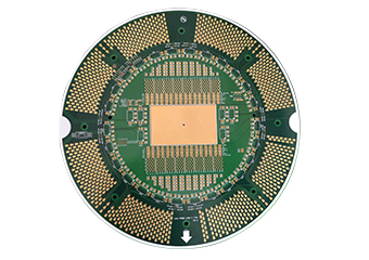
Thick copper plate/bare copper plate thermal conductivity 2-3W
★ Thermoelectric separation process, 100% computer open and short circuit test
★ High heat dissipation performance, used for radiators, power supplies, etc.
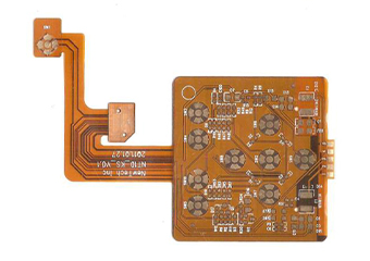
1~8 layers of rolled copper/electrolytic copper
★ Raw material Shengyi, Taihong and other brands have guaranteed quality
★ It can be used for soft and hard combination, FPC multi-layer board, cable, etc.
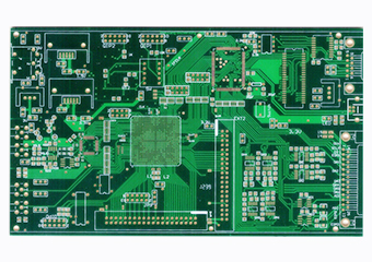
High precision PCB board
Minimum line width and line spacing 3/3mil minimum via 0.15mm
★ It can be used as solder mask bridge and via hole plugging technology
★ There are impedance requirements, electric golden fingers, precise lines, etc.
Number | Project | Content |
1. | Layers | Single-sided/double-sided/multi-layer (4-32 layers) |
2. | Material | Common: FR-4 (Medium TG High TG), CEM-1 Special: CEM-3, Rogers |
3. | Surface treatment process | Lead-free technology: lead-free HASL, immersion nickel gold, gold plating, organic solder protection film (OSP) |
4. | Special Process | 1. Impedance board (impedance requirement is within ±10%) 2. High copper thick plate (copper thickness of inner and outer layers is 3-4 OZ) 3. High TG board/halogen-free board/halogen-free high TG board |
5. | Processed plate thickness | 0.4-3.2mm |
6. | Processing size | Maximum processing size: 600MM X600MM Minimum processing size: 5MM X 5MM |
7. | Minimum aperture | 0.1mm |
8. | Minimum line width and line spacing | Minimum line width: 0.125mm Minimum line spacing: 0.125mm |
9. | Plate Thickness Aspect Ratio | 1:8 within |
10. | Minimum annular ring | 0.2mm |
11. | Outer copper thickness | 18μm、35μm、70μm、 105μm、140μm |
12. | Solder mask oil film type | Liquid Photosensitive Solder Resist Ink |
13. | Solder resist ink color | Photosensitive series: green, black, red, yellow, white, blue, orange, etc. Matt series: green, black sun ink |
14. | Shape processing method | Die stamping、CNC |
15. | Tolerance | Line width ± 10%, aperture + 3Mil, shape processing ± 0.15MM (special process to be determined separately) |
16. | Coating thickness | 1. HASL: copper thickness 18-25um, tin thickness 5-40um 2. Immersion gold plate: nickel thickness 2.5-5μm, gold thickness 0.05-0.1μm 3. OSP board: film thickness 0.2-0.5um |
17. | Warpage | ≤0.75% |

21 лет опыта в производстве тарелок

Тысячи клиентов по всему миру

Тонкое мастерство

Своевременная доставка
WeChat
Отсканируйте QR-код с помощью WeChat